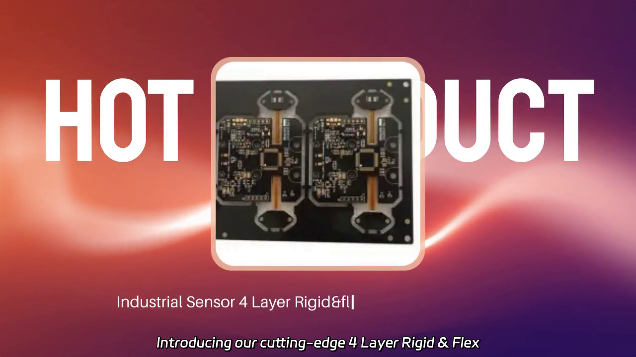
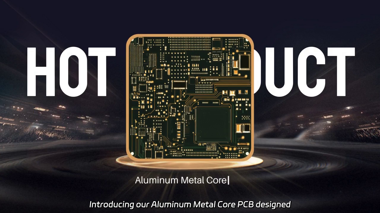
In today's fast-paced world of electronics, the demand for high-density interconnect (HDI) technologies is on the rise. HDI PCBs utilize advanced design techniques, featuring smaller vias, fine lines, and controlled impedance, all contributing to outstanding performance and increased circuit density. As products like laptops and mobile phones become more compact, the lightweight and miniaturized nature of HDI boards becomes a game changer, significantly reducing the risk of damage and ensuring reliability.
Engineers play a crucial role in the HDI manufacturing process, requiring meticulous attention to detail and exceptional soldering skills. With unique characteristics such as microvias and blind vias, these printed circuit boards not only enhance performance but also support sophisticated applications in a shrinking physical footprint. Join us as we explore the innovative world of HDI PCB design and its impact on the future of technology!
Engineers play a crucial role in the HDI manufacturing process, requiring meticulous attention to detail and exceptional soldering skills. With unique characteristics such as microvias and blind vias, these printed circuit boards not only enhance performance but also support sophisticated applications in a shrinking physical footprint. Join us as we explore the innovative world of HDI PCB design and its impact on the future of technology!